| |
Introduction to Wound Chip Inductors
Wound chip inductors are the most popular inductive components. They offer a wide range of inductance values and current handling capacity. They are ideal for replacing thru-hole RF inductors that have been used for many years in all types of electronic circuits.
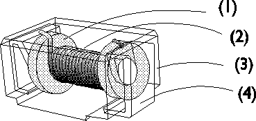
Construction of Wound Molded Chip Inductors
- Core:
High stability ferrite core
- Wire:
Hi-temp polyurethane copper wire
- Electrode terminal:
High condition, heat resistant copper alloys
- Mold enclosure:
Low stress epoxy resin
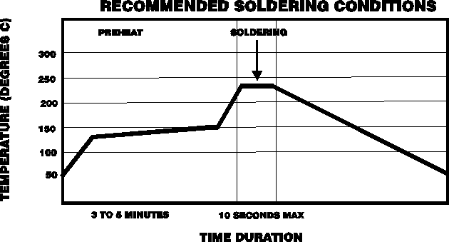
Soldering
All chip inductors should be pre-heated at a temperature of 120° C to 150° C for three to five minutes. Flow and reflow soldering should be done at 230° C for less than ten seconds. If using soldering iron, the temperature at the tip of the soldering iron should not exceed 350° C. Re-soldering with soldering iron is not recommended. It is recommended that copper wire non-corrosive flux be used. Be careful of pH and of the amount of chlorine in the flux. Make sure it does not spread to the surface of the board. After soldering, chip inductors should not be stressed excessively.
Testing
We measure L & Q with an HP4192A, HP4191A impedance analyzer and spring test fixture HP16092A, or with an HP4195A network analyzer. SRF and IDC are measured with an HP4191A or HP4195A. DC resistance is measured with digital multimeter SC7401 or an HP3478A. All tests have been performed at the temperature of 20° C plus or minus 2° C with relative humidity of 65% (± 5%).
Cleaning
Do not use ultrasonic cleaning. We recommend vapor degreasing and water detergent rinse as preferred cleaning methods. Organic solvents also may be used.
Storage
Chip inductors should not be stored under high temperature and high humidity conditions. Specifically, do not store reels of chip inductors in an area exposed to heat or direct sunlight. This may cause packaging material to become deformed, causing problems during mounting.
Mounting
Placement force should not exceed 5 pounds. If more than 5 pounds is used, it may cause a change in electric and magnetic characteristics. High component mounting densities may degrade solder adhesion performance in flow soldering. In such a situation, care should be given to degassing (flux gases).
Pattern Design
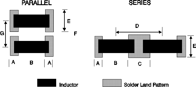
- Recommended land pattern for IC0603 is from 0.8 mm to 1.2 mm.
- Recommended land pattern for IC0805 is from 1.2 mm to 1.4 mm.
- Recommended land pattern for IC1008 is from 2.0 mm to 2.6 mm.
- Recommended land pattern for IC1210 is from 2.4 mm to 3.0 mm.
- Recommended land pattern for IC1812 is from 3.2 mm to 4.0 mm.
Avoid placing inductor over any metal pattern such as interconnect lines or traces. This may cause a change in inductance value, reduction in Q and generate mutual inductance.
Land Pattern Design for Molded and Shielded Wound Chip Inductors. Dimensions in mm.
(Please consult factory for updates to these dimensions)
| Size |
A |
B |
C |
D |
E |
F |
G |
| IC0603 |
0.8 |
0.8 |
1.8 |
2.6 |
1.2 |
0.2 |
1.4 |
| IC0805 |
1.0 |
1.0 |
2.2 |
3.2 |
1.4 |
0.2 |
1.6 |
| IC1008 |
1.0 |
1.5 |
2.6 |
4.1 |
2.6 |
0.4 |
3.0 |
| IC1210 |
1.0 |
2.2 |
3.0 |
5.2 |
3.0 |
0.5 |
3.5 |
| IC1812 |
1.5 |
3.0 |
3.5 |
6.5 |
4.0 |
0.6 |
4.6 |
Wound Chip Inductor Reliability Tests
| Item |
Requirement |
Test Methods |
| Dielectric withstanding voltage |
No evidence of fuming, flaming or breakdown |
5 seconds at DC 1000 volts between both terminals and package |
| Insulation resistance |
1000 Mohm and over |
1 minute at DC 500 volts measured between both terminals and package |
| Terminal pull strength |
No evidence of breakdown |
Terminal should withstand a pull force of 1 Kg in a horizontal direction |
| Terminal bend strength |
No evidence of breakdown |
Inductor should be soldered on PCB and supported by applying strength so that the bending width becomes 10 mm |
| Vibration |
Inductance should be within 3% of initial measurement |
2 hours in each direction of X, Y, Z, on PCB at a frequency range of 10-55-10 MHz with 1.5 mm amplitude |
| Dropping |
No evidence of damage, L should be within 3% of initial measurement |
Dropping from 1 m on to a concrete surface 3 times |
| Resistance to soldering heat |
No evidence of damage, L should be within 3% of initial measurement |
Immerse inductor in solder (63/37) @ 260° C ±5° C for 10 ±1 second |
| Solderability |
Approximately 95% of the terminal should be covered with new solder |
Immerse inductor in the solder (63/37) @ 230° C ±5° C for 3 ±0.5 seconds |
| Thermal shock |
No evidence of damage; delta L/L within ±5%, delta Q/Q within ±20% |
100 cycles between −25° C in 1 hour and +100° C in 1 hour |
| Temperature characteristics |
Inductance should be within 10% of initial value |
Inductance to be measured at the temperature of between −25° C and +85° C based on the ambient temperature of 20° C |
| Moisture endurance |
No evidence of damage; delta L/L within ±5%, delta Q/Q within ±30% |
Test at temperature of 40° C ±2° C, humidity 90-95% for 1000 hours |
| Resistance to solvents |
Marking is clearly visible, no damage |
MIL-STD-202, method 215 |
| Low temperature characteristics |
No evidence of damage; delta L/L within ±5%, delta Q/Q within ±20% |
Store at −40° C ±2° C for 1000 hours |
|