Introduction to Multilayer Surface Mount Inductors
Multilayer chip inductors were introduced in 1987 and soon became the inductive components of choice for many design engineers. Multilayer technology offers three advantages:
- Monolithic structure — excellent for high reliability
- Magnetic shielding — outstanding for very high density applications
- Low mounting cost
Construction of Multilayer Chip Inductors
Multilayer chip inductors do not require winding. They consist of ferrite paste and conductive paste alternately layered and sintered in a monolithic structure. The process can be described as follows:
- First a ferrite paste and a conductive paste are printed. This is the starting point of the conductor.
- Another ferrite paste and conductive paste are printed, and connected to the conductor pattern.
- Another ferrite paste and conductive paste are printed, completing the conductor pattern.
- Last ferrite paste is printed.
- Co-firing.
- Terminal / electrode processing.
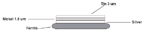
Terminal Electrode Construction
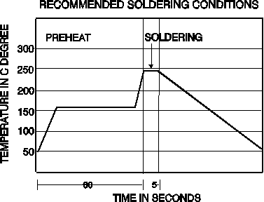
Soldering
Multilayer chip inductors are designed for flow or reflow soldering methods only. All chips should be pre-heated at a temperature of 150° C for 60 seconds. Flow and reflow should be done at 260° C for 5 seconds, with rosin flux (chlorine less than 0.20% wt.).
If using soldering iron, the following conditions must be met:
- Soldering iron — 30 Watts maximum
- Tip temperature — 300° C maximum
- Soldering time — 3 to 5 seconds maximum
Testing
We use:
- Impedance Analyzer HP4291A with test fixture HP16192A to test for Z, DCR, XI
- HP6632A DC Power Supply connected to HP16200A adapter, then connected to HP4291A to add DC current bias.
All tests should be performed at 20° C ±2° C and with relative humidity at 65% (±5%).
Cleaning
Vapor degreasing and water detergent rinse are the cleaning methods we recommend. Be sure to completely remove all flux residue. Some cleaning agents may change the color of the chip body to slightly white; however, product performance is not affected.
For additional help with cleaning components, contact ACT’s engineering department.
Storage
All multilayer chips should be stored on tape and reel. We do not recommend bulk storage of these parts. Do not expose reels to prolonged heat or direct sunlight. Do not store in relative humidity higher than 65%. Avoid areas that have sudden changes in temperature and humidity. Do not store components in a chemical atmosphere such as chlorine gas, acid or sulfide gas.
Land Pattern Design
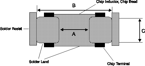
Land Pattern Design. Dimensions in mm.
Land Pattern
Recommendation |
0603 |
0805 |
1206 |
1210 |
1806 |
1812 |
SWB |
| A |
0.8 |
1.2 |
2.0 |
2.0 |
3.0 |
3.0 |
4.0 |
| B |
2.4 to 3.4 |
3.0 to 4.0 |
4.2 to 5.2 |
5.5 to 6.5 |
5.5 to 6.5 |
5.5 to 6.5 |
7.4 to 8.4 |
| C |
0.6 |
1.0 |
1.2 |
1.8 |
1.2 |
2.4 |
4.0 |
Testing
- L and Q, we use HP4291A with test fixture HP16192A or HP4195A network analyzer
- DCR, we use HP4338A or SC7401 digital multimeter
- Rated current, we use HP4291A with HP16200A Adapter, and HP6632A power supply
Mechanical Performance Test
| Item |
Specification |
Test Condition |
| Solderability |
More than 90% of the terminal electrode should be covered with solder. |
Preheat: 120° C to 150° C for 60 seconds.
Solder type: H63A (63/37 Eutectic solder).
Solder temp: 230° C ±5° C. Flux: rosin non RH.
Dip time: 10 ±1 second. |
| Solder heat resistance |
No change in appearance.
No cracks.
No change in performance.
90% of terminal is covered with solder. |
Same test conditions as above. |
| Terminal strength |
No evidence of breakdown.
No damage to either body or terminal of the bead. |
- 0603: 0.5 Kgf @ 30 ±5 seconds
- 0805: 0.6 Kgf @ 30 ±5 seconds
- 1206: 1.0 Kgf @ 30 ±5 seconds
- 1210: 1.0 Kgf @ 30 ±5 seconds
- 1806: 1.0 Kgf @ 30 ±5 seconds
- 1812: 1.5 Kgf @ 30 ±5 seconds
|
| Bending strength |
No evidence of damage |
- 0603: 1.0 A(mm) and 0.5 Kgf
- 0805: 1.4 A(mm) and 1.0 Kgf
- 1206: 2.0 A(mm) and 2.0 Kgf
- 1210: 2.0 A(mm) and 2.5 Kgf
- 1806: 2.5 A(mm) and 2.5 Kgf
- 1812: 2.7 A(mm) and 2.5 Kgf
|
Environmental Performance Test
| Thermal shock (temperature cycle) |
Temperature 50 cycles between −25° C for 1 hour and +85° C for 1 hour |
| Humidity resistance |
Temperature: +60° C
Humidity: 90% RH
Applied current: 200 mA/DC
Time: 500 hours |
| High temperature resistance |
Temperature: +80° C
Applied current: 200 mA/DC
Time: 500 hours |
Note: All measurements are performed at room temperature, 24 hours after test. Impedance should be within 20% of initial value. There should be no evidence of damage.
ACT’s Commitment to EMI Suppression Components
Since the demand for EMI supression components is increasing, we at ACT have focused our R&D effort toward the development of a variety of new EMI suppressors. We now offer “off-the-shelf” solutions for noise suppression, which spare you the hassle of dealing with multiple suppliers — and also save you time in design and product development.
Our EMI suppression components comprise multilayer chip beads, shielded beads, line filters, common mode chokes; EMI ferrites for high and very high frequency applications — even coupled with high current handling (up to 8 amps) and high impedance (up to 10,000 ohms). Dimensions and styles also are offered in great variety. Should you need them, we can produce custom products at prices comparable to those of standard products.
To provide the highest quality components possible and to increase our QC efficiency, we have incorporated new, state-of-the-art test equipment.
Our engineering department is available to answer your questions about EMI suppression components. We can supply product sample kits designed to help you evaluate relevant products within our line. |